Bulk GaN -
Advanced substrate material for device
fabrication
First True Bulk
GaN
SCSA, Inc. proudly
announces fabrication of the First True Bulk
GaNcrystals
This is a breakthrough achievement in scsa’s program to develop GaN
substrate fabrication technology.
Fabrication process consists of the following
steps:
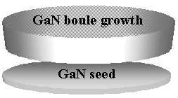
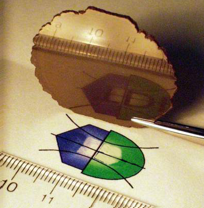
Step 1: Bulk GaN boule growth on GaN seed
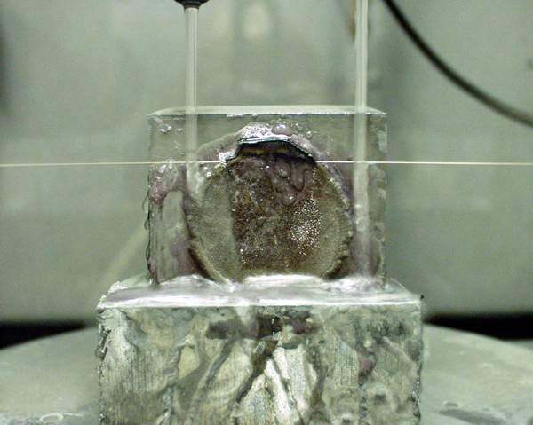
Step 2 : Slicing of the grown boule into wafers (35 mm diameter GaN boule sliced by a diamond wire saw is
shown)
Step 3 : Polishing of GaN wafers
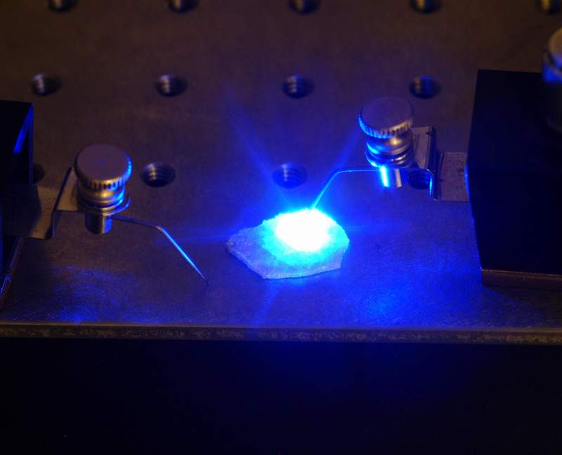
LED fabricated on SCSA’s bulk GaN substrate. One of the electrodes is placed on top of the LED
structure and the other one is connected to conducting GaN
substrate.
Bulk GaN substrates are not available yet commercially
Please, contact Wafer Mart for further information
등록된 제품이외의 사양으로 원하시면 견적요청을
이용하여 주시거나
비슷한 모델에 자세한 내용을 기재하여 견적요청을 하여 주십시오.