Applications
- GaN Epitaxial
Wafers may be used as substrates for III-V nitride epitaxial growth by MBE, MOCVD and CVD.
- No buffer layer is
required.
- GaN Epitaxial
Wafers are the ideal substrates for GaN homoepitaxial growth and device
manufacturing.
Technology
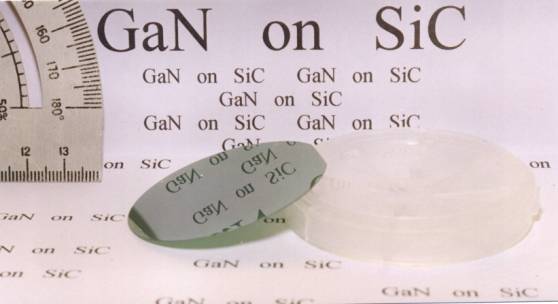
Gallium Nitride Epitaxial
Wafer (template) consists of a thin undoped GaN epitaxial layer grown by Hydride
Vapor Phase
Epitaxy (HVPE) directly on (0001)Si face on-axis 6H-SiC or 4H-SiC
substrate.
Additional
information
GaN layers and SiC substrates
are electrically conducting. Silicon carbide insures excellent heat removal
from nitride
device structure, which is important for high-power devices.
GaN/SiC wafers may be cleaved providing mirror-like facets
for nitride laser
diodes.
GaN
layers could be grown on SiC substrates supplied by customers.
|